LTC4214-1/LTC4214-2
19
421412f
tween the compensation capacitor C
C
and the MOSFETs
C
ISS
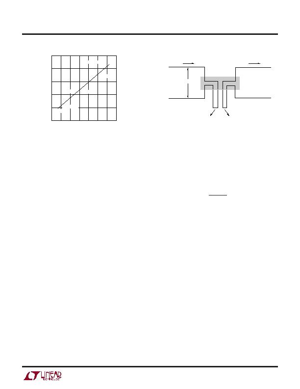
. The line in Figure 6 is used to select a starting value
for C
C
based upon the MOSFETs C
ISS
specification. Opti-
mized values for C
C
are shown for several popular
MOSFETs. Differences in the optimized value of C
C
versus
the starting value are small. Nevertheless, compensation
values should be verified by board level short-circuit
testing.
As seen in Figure 5 previously, at the onset of a short-
circuit event, the input supply voltage can ring dramati-
cally owing to series inductance. If this voltage avalanches
the MOSFET, current continues to flow through the MOSFET
to the output. The analog current limit loop cannot control
this current flow and therefore the loop undershoots. This
effect cannot be eliminated by frequency compensation. A
zener diode is required to clamp the input supply voltage
and prevent MOSFET avalanche.
SENSE RESISTOR CONSIDERATIONS
For proper circuit breaker operation, Kelvin-sense PCB
connections between the sense resistor and the LTC4214s
V
EE
and SENSE pins are strongly recommended. The
drawing in Figure 7 illustrates the correct way of making
connections between the LTC4214 and the sense resistor.
PCB layout should be balanced and symmetrical to mini-
mize wiring errors. In addition, the PCB layout for the
sense resistor should include good thermal management
techniques for optimal sense resistor power dissipation.
TIMING WAVEFORMS
System Power-Up
Figure 8 details the timing waveforms for a typical power-
up sequence in the case where a board is already installed
in the backplane and system power is applied abruptly. At
time point 1, the supply ramps up, together with UV/OV,
V
IN
, V
OUT
, DRAIN and PWRGD. At time point 2, V
IN
exceeds V
LKO
and the internal logic checks for UV > V
UVHI
,
OV < V
OVHI
, GATE < V
GATEL
, SENSE < V
CB
, SS < 20 " V
OS
and TIMER < V
TMRL
. If all conditions are met, an initial
timing cycle starts and the TIMER capacitor is charged by
a 5礎 current source pull-up. At time point 3, TIMER
reaches the V
TMRH
threshold and the initial timing cycle
terminates. The TIMER capacitor is quickly discharged. At
time point 4, the V
TMRL
threshold is reached and the
conditions of GATE < V
GATEL
, SENSE < V
CB
and
SS < 20 " V
OS
must be satisfied before a GATE ramp-up
cycle begins. SS ramps up as dictated by R
SS
" C
SS
(as in
Equation 6); GATE is held low by the analog current limit
(ACL) amplifier until SS crosses 20 " V
OS
. Upon releasing
GATE, 50礎 sources into the external MOSFET gate and
compensation network. When the GATE voltage reaches
the MOSFETs threshold, current begins flowing into the
load capacitor at time point 5. At time point 6, load current
reaches the SS control level and the analog current limit
loop activates. Between time points 6 and 8, the GATE
voltage is servoed, the SENSE voltage is regulated at
V
ACL
(t) (Equation 7) and soft-start limits the slew rate of
APPLICATIO S I FOR ATIO
U
U
U
W
CURRENT FLOW
FROM LOAD
CURRENT FLOW
TO 12V BACKPLANE
SENSE RESISTOR
TRACK WIDTH W:
0.03" PER AMP
ON 1 OZ COPPER
TO
SENSE
TO
V
EE
4214 F07
Figure 7. Making PCB Connections to the Sense Resistor
Figure 6. Recommended Compensation
Capacitor C
C
vs MOSFET C
ISS
MOSFET, C
ISS
(pF)
0 1000
0
10
25
2000
4000 5000
4214 F06
5
20
15
3000
6000 7000
"
"
"
"
"
"
IRF7803
Si4412ADY
Si4410DY
Si4876DY
Si4864DY
IRF7413
发布紧急采购,3分钟左右您将得到回复。
相关PDF资料
LTC4215IUFD#PBF
IC CNTRLR HOT SWAP 24-QFN
LTC4216IDE#TRPBF
IC CNTRLR HOT SWAP 12-DFN
LTC4221IGN#TRPBF
IC CTRLR HOTSWAP DUAL 16SSOP
LTC4222CG#PBF
IC CTRLR DUAL HOT SWAP 36-SSOP
LTC4223CDHD-2#PBF
IC CNTRLR HOT SWAP DUAL 16-DFN
LTC4224IDDB-2#TRPBF
IC CNTRLR HOT SWAP DUAL 10-DFN
LTC4225IGN-1#PBF
IC CONTROLLER HOT SWAP 24-SSOP
LTC4230CGN#TRPBF
IC CONTRLLR HOT SWAP TRPL 20SSOP
相关代理商/技术参数
LTC4214-2CMS
功能描述:IC CTRLR HOTSWAP NEGVOLT 10MSOP RoHS:否 类别:集成电路 (IC) >> PMIC - 热交换 系列:- 标准包装:50 系列:- 类型:热交换控制器 应用:-48V 远程电力系统,AdvancedTCA ? 系统,高可用性 内部开关:无 电流限制:可调 电源电压:11.5 V ~ 14.5 V 工作温度:-40°C ~ 85°C 安装类型:表面贴装 封装/外壳:10-TFSOP,10-MSOP(0.118",3.00mm 宽) 供应商设备封装:10-MSOP 包装:管件
LTC4214-2CMS#PBF
功能描述:IC CTRLR HOTSWAP NEGVOLT 10MSOP RoHS:是 类别:集成电路 (IC) >> PMIC - 热交换 系列:- 标准包装:50 系列:- 类型:热交换控制器 应用:-48V 远程电力系统,AdvancedTCA ? 系统,高可用性 内部开关:无 电流限制:可调 电源电压:11.5 V ~ 14.5 V 工作温度:-40°C ~ 85°C 安装类型:表面贴装 封装/外壳:10-TFSOP,10-MSOP(0.118",3.00mm 宽) 供应商设备封装:10-MSOP 包装:管件
LTC4214-2CMS#TR
功能描述:IC CONTROLLER HOTSWAP NEG 10MSOP RoHS:否 类别:集成电路 (IC) >> PMIC - 热交换 系列:- 标准包装:50 系列:- 类型:热交换控制器 应用:-48V 远程电力系统,AdvancedTCA ? 系统,高可用性 内部开关:无 电流限制:可调 电源电压:11.5 V ~ 14.5 V 工作温度:-40°C ~ 85°C 安装类型:表面贴装 封装/外壳:10-TFSOP,10-MSOP(0.118",3.00mm 宽) 供应商设备封装:10-MSOP 包装:管件
LTC4214-2CMS#TRPBF
功能描述:IC CTRLR HOTSWAP NEGVOLT 10MSOP RoHS:是 类别:集成电路 (IC) >> PMIC - 热交换 系列:- 产品培训模块:Obsolescence Mitigation Program 标准包装:100 系列:- 类型:热插拔开关 应用:通用 内部开关:是 电流限制:可调 电源电压:9 V ~ 13.2 V 工作温度:-40°C ~ 150°C 安装类型:表面贴装 封装/外壳:10-WFDFN 裸露焊盘 供应商设备封装:10-TDFN-EP(3x3) 包装:管件
LTC4214-2IMS
功能描述:IC CONTROLLER HOTSWAP NEG 10MSOP RoHS:否 类别:集成电路 (IC) >> PMIC - 热交换 系列:- 产品培训模块:Obsolescence Mitigation Program 标准包装:100 系列:- 类型:热插拔开关 应用:通用 内部开关:是 电流限制:可调 电源电压:9 V ~ 13.2 V 工作温度:-40°C ~ 150°C 安装类型:表面贴装 封装/外壳:10-WFDFN 裸露焊盘 供应商设备封装:10-TDFN-EP(3x3) 包装:管件
LTC4214-2IMS#PBF
功能描述:IC CTLR HOTSWAP NEGVOLT 10MSOP RoHS:是 类别:集成电路 (IC) >> PMIC - 热交换 系列:- 产品培训模块:Obsolescence Mitigation Program 标准包装:100 系列:- 类型:热插拔开关 应用:通用 内部开关:是 电流限制:可调 电源电压:9 V ~ 13.2 V 工作温度:-40°C ~ 150°C 安装类型:表面贴装 封装/外壳:10-WFDFN 裸露焊盘 供应商设备封装:10-TDFN-EP(3x3) 包装:管件
LTC4214-2IMS#TR
功能描述:IC CONTROLLER HOTSWAP NEG 10MSOP RoHS:否 类别:集成电路 (IC) >> PMIC - 热交换 系列:- 产品培训模块:Obsolescence Mitigation Program 标准包装:100 系列:- 类型:热插拔开关 应用:通用 内部开关:是 电流限制:可调 电源电压:9 V ~ 13.2 V 工作温度:-40°C ~ 150°C 安装类型:表面贴装 封装/外壳:10-WFDFN 裸露焊盘 供应商设备封装:10-TDFN-EP(3x3) 包装:管件
LTC4214-2IMS#TRPBF
功能描述:IC CTRLR HOTSWAP NEGVOLT 10MSOP RoHS:是 类别:集成电路 (IC) >> PMIC - 热交换 系列:- 产品培训模块:Obsolescence Mitigation Program 标准包装:100 系列:- 类型:热插拔开关 应用:通用 内部开关:是 电流限制:可调 电源电压:9 V ~ 13.2 V 工作温度:-40°C ~ 150°C 安装类型:表面贴装 封装/外壳:10-WFDFN 裸露焊盘 供应商设备封装:10-TDFN-EP(3x3) 包装:管件